Intel Core I7 Processor
Published on Aug 15, 2016
Abstract
Intel core i7 is a family of three Intel desktop processor, the first processor released using the Intel Nehalem micro architecture and the successor to the Intel Core 2 family. All three models are quad core processors.
A quad core processor consists of four cores. Quad core technology is a type of technology that includes two separate dual-core dies, where dual-core means a CPU that includes two complete execution cores per physical processor, installed together in one CPU package. In this setup cores 1 and 2 would share a memory cache, and core 3 and 4 another cache. Communication between core 1 and 2 and core 3 and 4 using QPI(Quick Path Interconnect)
They are 64 bit processors. In computer architecture, 64-bit integers, memory addresses, or other data units are those that are at most 64 bits (8 octets) wide. Also, 64-bit CPU and ALU architectures are those that are based on registers, address buses, or data buses of that size.
The need for core i7 processors requires a comparison with their immediate predecessors. The comparison can be summarized as follows. The Core i7 is a completely new architecture which is much faster and more efficient than the Core 2 Duo. Currently only the Core i7 920, 945 and 965 XE versions are available. Of that the Core i7 920 is available at just $284 which makes it a great buy. It offers better performance than almost all Core 2 Duo processors
Introduction of Intel Core I7 Processor
A cpu socket or cpu slot is an electrical component that attaches to a circuit board and is designed to house a cpu. It is a special type of IC socket designed for very high pin counts. A cpu socket provides many functions including providing a physical structure to support the cpu, facilitating replacement and cost reduction and as an electrical interface both with the cpu and the circuit board.
Core i7 uses an LGA1366 socket.(socket B). it is incompatible with the previous versions. LGA refers to Land Grid Array and is used as a physical interface for microprocessors of the Intel Pentium 4, Intel Xeon, Intel Core 2 and AMD Opteron families. Earlier the socket used was the PGA(Pin Grid Array). In LGA there are no pins on the chip .Instead there are pads of gold plated copper that touch pins on the motherboard. LGA provides a larger contact point, allowing for eg higher clock frequencies. It also allows higher pin densities and thus enables a more stable power supply to the chip
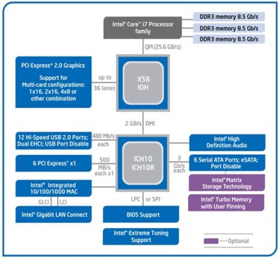
The memory is directly connected to the processor. The memory is divided into three channels. Each channel can support one or two DDR3 RAMs. Motherboards for core i7 have three or six RAM slots.DDR3 RAM is double data rate 3 random access memory. This is a RAM technology used for high speed storage of the working data of a computer or other digital electronic devices. The primary benefit of DDR3 is its ability to run its I/O bus at four times the speed of the memory cells contained in it. It enables faster bus speeds and higher throughputs than earlier memory technologies. There is a significant reduction in the power consumption. It needs only 1.5V compared to 1.8V for DDR2
HOW IT WORKS:
The instruction decoder has three decoder units that can decode one simple instruction per cycle per unit. The other decoder unit can decode one instruction every cycle, either simple instruction or complex instruction made up of several micro-ops.Instructions made up of more than four micro-ops are delivered from the MSROM. Upto four micro-ops can be delivered each cycle to the instruction decoder queue (IDQ).The IDQ delivers micro-op stream to the allocation/renaming stage of the pipeline.
The out-of-order engine supports up to 128 micro-ops in flight. Each micro-ops must be allocated with the following resources: an entry in the re-order buffer (ROB), an entry in the reservation station (RS), and a load/store buffer if a memory access is required.The allocator also renames the register file entry of each micro-op in flight. The inputdata associated with a micro-op are generally either read from the ROB or from theretired register file.
The RS dispatch up to six micro-ops in one cycle if the micro-ops are ready to execute. The RS dispatch a micro-op through an issue port to a specific execution cluster, each cluster may contain a collection of integer/FP/SIMD execution units.The result from the execution unit executing a micro-op is written back to the register file, or forwarded through a bypass network to a micro-op in-flight that needs the result. Intel microarchitecture (Nehalem) can support write backthroughput of one register file write per cycle per port. The bypass network consistsof three domains of integer/FP/SIMD. Forwarding the result within the same bypass domain from a producer micro-op to a consumer micro is done efficiently in hardware without delay.
Forwarding the result across different bypass domains may be subject to additional bypass delays. The bypass delays may be visible to software in addition to the latency and throughput characteristics of individual execution units.Intel microarchitecture (Nehalem) contains an instruction cache, a first-level datacache and a second-level unified cache in each core.
Each physical processor may contain several processor cores and a shared collection of subsystems that are referred to as "uncore". Specifically in Intel Core i7 processor, the uncore provides a unified third-level cache shared by all cores in the physical processor, Intel QuickPath Interconnect links and associated logic. The L1 and L2 caches are writeback and non-inclusive.The shared L3 cache is writeback and inclusive, such that a cache line that exists ineither L1 data cache, L1 instruction cache, unified L2 cache also exists in L3. The L3 is designed to use the inclusive nature to minimize snoop traffic between processor cores. The latency of L3 accessmay vary as a function of the frequency ratio between the processor and the uncore sub-system