Asynchronous Chips
Published on Dec 16, 2015
Abstract
Computer chips of today are synchronous. They contain a main clock, which controls the timing of the entire chips. There are problems, however, involved with these clocked designs that are common today.One problem is speed. A chip can only work as fast as its slowest component.
Therefore, if one part of the chip is especially slow, the other parts of the chip are forced to sit idle. This wasted computed time is obviously detrimental to the speed of the chip.
New problems with speeding up a clocked chip are just around the corner. Clock frequencies are getting so fast that signals can barely cross the chip in one clock cycle. When we get to the point where the clock cannot drive the entire chip, we'll be forced to come up with a solution. One possible solution is a second clock, but this will incur overhead and power consumption, so this is a poor solution. It is also important to note that doubling the frequency of the clock does not double the chip speed, therefore blindly trying to increase chip speed by increasing frequency without considering other options is foolish.
The other major problem with c clocked design is power consumption. The clock consumes more power that any other component of the chip. The most disturbing thing about this is that the clock serves no direct computational use. A clock does not perform operations on information; it simply orchestrates the computational parts of the computer.
New problems with power consumption are arising. As the number of transistors on a chi increases, so does the power used by the clock. Therefore, as we design more complicated chips, power consumption becomes an even more crucial topic. Mobile electronics are the target for many chips.
These chips need to be even more conservative with power consumption in order to have a reasonable battery lifetime.The natural solution to the above problems, as you may have guessed, is to eliminate the source of these headaches: the clock.
DISCUSSION
Asynchronous, or clock less, design has advantages over the synchronous design.
The first of these advantages is speed. Chips can run at the average speed of all its components instead of the speed of its slowest component, as was the case with a clocked design. Also the need to have a clock running at a speed such that the signal can reach all parts of the chip is eliminated. Therefore, the speed of an asynchronous design is not limited by the size of the chip.
An example of how much an asynchronous design can improve speed is the asynchronous Pentium designed by Intel in 1997 that runs three times as fast as the synchronous equivalent. This speedup is certainly significant and proves the usefulness of a clock less design.
The other advantage of a clock less design is power consumption.
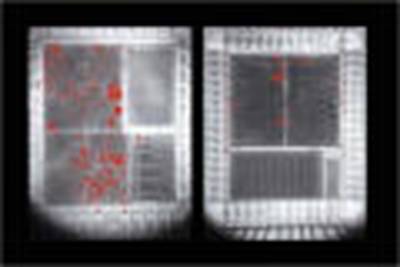
Special light emission measurements of a synchronous chip (left) and an asynchronous chip (right) with the same digital functionality under the same operational conditions indicate hoe much power the chips dissipate.
The above graphic illustrates the power saving characteristic of a clock less design. The reason for this is that asynchronous chips use power only during computations, while a clocked chip always consumes power because the chip is always running. Remember that the clock is the component which consumes the most power. Therefore, eliminating the clock eliminates the largest component of power consumption.
One example of improved power consumption is the same Intel Pentium asynchronous chip. This design, which ran up to three times as fast as the clocked version, runs on half the power of the clocked version. This is incredible support for a clock less design. A second example of improved power consumption is a Philips prototype chip that runs on one-third of the power of its clocked counterpart.
Clock less design is inevitable in the future of chip design because of the two major advantages of speed and power consumption, but where will we first see these designs in use?
The first place we’ll see, and have already seen, clock less designs are in the lab. Many prototypes will be necessary to create reliable designs. Manufacturing techniques must also be improved so the chips can be mass-produced.
The second place we’ll see these chips are in mobile electronics. This is an ideal place to implement a clock less chip because of the minimal power consumption. Also, low levels of electromagnetic noise creates less interference, less interference is critical in designs with many components packed very tightly, as is the case with mobile electronics.
The third place is in personal computers (PCs). Clock less designs will occur here last because of the competitive PC market.
It is essential in that market to create an efficient design that is reasonably priced. A manufacturing cost increase of a couple of cents per chip can cause an entire line of computers to fail because of the large cost increase passed onto the customer. Therefore, the manufacturing process must be improved to create a reasonably priced chip.
A final place that asynchronous design may be used is encryption devices. The reason for this is there are no regularly timed signals for hackers to look for. This becomes even more critical as computers all over the world become more closely connected and are sharing confidential material. Security in the United States has increased greatly in recent times; therefore, a clock less design will be welcomed because of its encryption abilities.
In summary, clock less designs have limitations, specifically a limited speed and high power consumption. Fortunately, these limitations can be solved with a clock less design. These asynchronous designs will be seen in many areas of technology, but it will take time before these chips can be perfected.
ASYNCHRONOUS LOGIC
Data-driven circuits design technique where, instead of the components sharing a common clock and exchanging data on clock edges, data is passed on as soon as it is available. This removes the need to distribute a common clock signal throughout the circuit with acceptable clock skew. It also helps to reduce power dissipation in CMOS circuits because gates only switch when they are doing useful work rather than on every clock edge.
There are many kinds of asynchronous logic. Data signals may use either “dual rail encoding” or “data building”. Each dual rail encoded Boolean is implemented as two wires. This allows the value and the timing information to be communicated for each data bit. Bundled data has one wire for each data bit and another for timing. Level sensitive circuits typically represent a logic one by a high voltage and a logic zero by a low voltage whereas transition signaling uses a change in the signal level to convey information. A speed independent design is tolerant to variations in gate speeds but not to propagation delays in wires; a delay insensitive circuit is tolerant to variations in wire delays as well.
The purest form of circuit is delay-insensitive and uses dual-rail encoding with transition signaling. A transition on one wire indicates the arrival of a zero, a transition on the other the arrival of a one. The levels on the wires are of no significance. Such an approach enables the design of fully delay-insensitive circuits and automatic layout, as the delays introduced by the layout compiler can’t affect the functionality (only the performance). Level insensitive designs can use simpler, stateless logic gates but require a “return to zero” phase in each transition.
More Seminar Topics:
Handfree Driving, Handheld Computers, Holographic Versatile Disc, Internet Telephony Policy in INDIA, Efficient Implementation Of Cryptographically Useful Large Boolean Functions, Aeronautical Communication, An ATM With An Eye, Blast, Blu Ray Disc, Brain Chips, Brain Gate, Buffer Overflow Attack, CAPTCHA, Coherent Acoustics Coding System, Digistar, Digital Video Editing, DRM Software Radio, Dual Core Processor, DVD Technology, DWDM, Dynamically Reconfigurability Computing, E Bombs, 3D Audio and Acoustic Environment Modeling, 64-Bit Computing, 3- D IC's, A BASIC TOUCH-SENSOR SCREEN SYSTEMRelated Seminar Topics
- Acoustics
- Animatronics
- Asynchronous Chips
- BiCMOS Technology
- Bioinformatics
- Boiler Instrumentation and Controls