Silicon on Plastic
Published on Nov 23, 2015
Abstract
The plastic substrates are thinner, lighter, shatterproof, flexible, rollable and foldable, making Silicon-on-Plastic an enabling technology for new applications/products. This paper studies the development of Silicon on Plastic technology.
Advances in poly-silicon technology have expanded TFT (THIN FILM TRANSISTORS) technology to high-speed electronics applications such as Smart Cards, RFID tags, portable imaging devices, photo-voltaic devices and solid-state lighting and other integrated circuit functions.
The challenge of Silicon-on-Plastic technology is to overcome the fact that plastic melts at the temperature required to build transistors in conventional TFT processes. Technological innovations have been made to accommodate silicon processing at low temperatures. T his paper describes an innovative ultra-low temperature poly-silicon TFT process on plastic substrates , Key technologies includes near room-temperature silicon and oxide deposition steps, laser crystallization and dopant activation. Manufacturing issues related to plastic material compatibility in a TFT process are reviewed. Lamination and de-lamination of plastic wafers to glass carrier wafers for manufacturability is discussed. An active matrix TFT backplane will be fabricated with an OLED (Organic Light Emitting Diode) display to demonstrate this technology.
Introduction of Silicon on Plastic
Currently, amorphous silicon thin film transistors (TFT's) on glass are predominantly used in the flat panel display industry for notebook computers, mobile phones, PDA's (Personal Digital Assistant), and other handheld devices. Today, flat panels made by amorphous TFT technology are replacing desktop computer CRT (Cathode Ray Tube) monitors at an ever-increasing rate. Amorphous TFT technology applications are limited due to its inherently low electron mobility.
Applications that require integration of display drivers such as hand-held camcorder and cell phone displays are using poly-silicon based TFT's for cost and space savings. This eliminates the need for costly assembly of conventional silicon chips onto the amorphous TFT display panels. Advances in poly-silicon technology have expanded TFT technology to high-speed electronics applications such as Smart Cards, RFID tags and other integrated circuit functions.
Recently developed ultra low-temperature polysilicon TFT technology can be applaid on both glass and plastic substrates. The plastic substrates are thinner, lighter, shatterproof, flexible, rollable and foldable, making silicon-on-plastic an enabling technology for new applications/products. Some of the possibilities are roll-up/down displays, lightweight, thin wall-mounted TVs, electronic newspapers, and wearable display/computing devices. Moreover, plastic substrates offer the potential of roll-to-roll (R2R) manufacturing which can reduce manufacturing cost substantially compared to conventional plate-to-plate (P2P) methods. Other possibilities include smart cards, RFID tags, and portable imaging devices, photo-voltaic devices and solid-state lighting.
The challenge of silicon-on-plastic technology is to overcome the fact that plastic melts at the temperature required to build transistors in conventional TFT processes. The ultra low-temperature process is compatible with plastic substrates and offers good TFT performance. Technological innovations have been made to accommodate silicon processing at low temperatures.
Low temperature (< 100º C) gate oxide deposition :
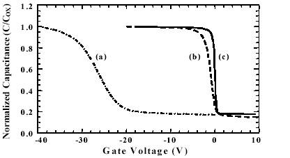
A proprietary deposition machine and a compatible process were developed to deposit high quality TFT gate oxides at sub-100º C temperatures. It is a special PECVD (Plasma-Enhanced Chemical Vapor Deposition) system with an added plasma source configuration akin to ECR (Electron Cyclotron Resonance) to generate high-density plasma at low temperature. The process is optimized to provide high-density plasma for silicon dioxide deposition using SiH4 and O2. The gate oxide film at 100 nm thickness has a breakdown voltage of more than 70V, while the gate leakage current density is less than 60 nA/cm2 at 20-V bias.As-deposited gate oxideshows good C-V characterstics .
1. A small amount of hysteresis is observed before annealing takes place. A pre-oxidation plasma treatment step using a mixture of H2 and O2 to grow a very thin oxide at the interface between the deposited silicon and the gate oxide with acceptable interface states was added to the process flow. Sufficiently high-density plasma must be generated in order to grow oxide with any significant thickness
. The chuck is cooled to 20º C to keep the plastic temperature below 100º C during the entire pre-oxidation and deposition process. The cleanliness of the Si surface is critical prior to the oxidation process.
The result exhibits the difference between gate oxides with and without pre-oxidation. With pre-oxidation, we obtain an oxide C-V curve very close to the one calculated theoretically.
A Xe-Cl excimer laser is used to crystallize sputtered silicon on plastic, thereby forming large polysilicon grains for TFT's with much higher mobility than its amorphous counterpart. The extremely short laser pulses provide sufficient energy to melt the deposited Si, while the subsequent cooling forms a polycrystalline structure. This crystallization technique is similar to polysilicon formation on glass. The challenge with plastic substrates is to melt the deposited silicon while preserving the structural quality of the underlying base material