IVY Bridge
Published on Nov 23, 2015
Abstract
The third generation of Intel Core processors microarchitecture codenamed Ivy Bridge, are released with quad-core models for both desktop and laptop computers. This introduces a new generation of optimization and new integrated graphics architecture support DirectX 11 which are one of the real news this generation. provides the latest technology for applications advanced, this quad-core processor features 8-core multitasking and additional L3 cache.
With excellent performance along with a speed incredible, also in this generation processors provides more intelligence to your PC, allowing applications and security protocols work great in the background. It has a screen resolution of most current and sharp thanks to technology Intel HD 2000 graphics integrated on the second generation Intel Core processors. This is a new generation 22nm optimization of existing models.
No introduction of new instructions or changes important in architecture except some optimizations and certainly important, a graph fully renovated in our tests has been pleasantly surprising. This generation also receives frequency increases and reductions of greater than 15% in four models cores. A major change that makes these models faster processors and more energetically efficient.
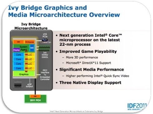
With the introduction of the Intel microarchitecture codenamed Sandy Bridge, the graphics processor has moved onto the same die as the CPU, and is now referred to as "processor graphics". In addition, processor graphics enjoys numerous architectural improvements that yield significant performance improvements over previous generations of Intel® integrated graphics parts. Ivy Bridge, provides another jump in functionality and performance over Sandy Bridge microarchitecture. Ivy Bridge microarchitecture is manufactured on the new 22nm process technology, incorporating Intel's new tri-gate (or 3D) transistor technology.
This innovative new process yields greater performance at much lower power. For example, the new tri-gate transistors exhibit 36% faster switching speed than the equivalent transistors on the legacy process at the same voltage. Tri-gate transistors also leak about 10x less current in their off state, resulting in a power saving of approximately 50% when using a comparable performance profile.
Although the Ivy Bridge microarchitecture has some significant differences from its predecessor Sandy Bridge, it's very easy to see that they are closely related to each other. There are in fact no differences at the very top.
The table below compares the main features for both Intel® HD Graphics 3000 found on the 2nd Generation Intel® CoreT processors and Intel® HD Graphics 4000 found on the 3rd Generation Intel® CoreT processors.
Series Chipset
The chipset that will support the IvyBridge takes some days with us. Specifically since April 8. That was its release date and now gave cover to SandyBridge processors since both processors share a 1155 socket contacts. In fact motherboards with chipsets sixth generation Ivy Bridge processors can be mounted with the updates appropriate bios. The same goes for the seventh generation that is Ivy Bridge oriented but also supports Sandy Bridge processors.
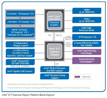
The Z77 chipset was the flagship model together with other similar variants as HM77 H77 or portable environments. We also find a B75aimed at business machines with the latest improvements in system vPro Intel. The main novelty of this chipset, in almost all its variables, is the integration of USB 3.0 natively (4 USB 3.0 ports and 12 USB 2.0 ports), becoming the first Intel chipset built with this technology, the settings are maintained for 6Gbps SATA two ports and four 3Gbps ports. It includes version 11 of Intel's RAID technology is added new graphics connective capacity through FDI dedicated bus, introduces enhancements for enterprise management systems (also for smaller IT departments), it adds support for the incorporation Thunderbolt, will improve energy saving systems, maintaining the legacy PCI supporting some versions and reduces the manufacturing process to 65nm.
CPU Speed
The Core i7-3770k model becomes the spearhead with a price similar to Core i7-2700K, but reducing consumption to 77W, the frequency are nailed(3.5GHz to 3.9GHz turbo mode), the cache is also the same (8MB), also the number of cores and all other associated technologies.
Of course the Core i7-3770k receives the new Intel graphics which is definitely an improvement important as it will allow us to achieve superior performance to models before and some additional tricks. addition, has features such as :
• The memory controller is integrated on the same processor.
• Three-channel memory (192-bit data width).
• The motherboard supports Intel Core i7 has four or six slots DIMM.
• Supports only DDR3
• Allows you to use the integrated DDR3 512 MB ??to 8 GB, you can also use 16 GB.
• FSB is replaced in the interface Quick Path i7 and i5.
• 731 million transistors (1,170 million in the Core i7 with 6 cores and12 MB ??of cache).
Instruction Set
The instruction set that works with Ivy Bridge Core i7 are the following:
• x86 : It is the generic name given to certain microprocessors from Intel family, their support and the basic architecture for these processors belong, by the end of their names numbers: 8086, 80286, 80386, 80486, etc.
• MMX : It is a SIMD instruction set designed by Intel and introduced in 1997 in their Pentium MMX microprocessors. It was developed from September 1 inserted in the Intel i860. It was supported by most manufacturers of x86 microprocessors since.MMX added 8 new records to the architecture, known as MM0to MM7 (hereinafter called MMn). Indeed, these new records are mere alias records x87 FPU stack. For whatever it is made ??with the FPU stack affects the MMX registers. Unlike the floating point stack, registers MMn are fixed instead of relative, so that can be accessed randomly.
• SSE : It is an extension to MMX instruction set processors Pentium III, introduced by Intel in February 1999. Instructions SSE are especially suitable for decoding MPEG2codec that is commonly used on DVD processing three-dimensional graphics and voice recognition software. These were initially known as "KNI" by Katmai New Instructions(Katmai was the codename of the first review of core Pentium III, Intel was interested in distinguishing its new line of previous generation processors, the Pentium II.
• SSE2 : It is one of the instruction sets of the IA-32 SIMD architecture. It was first used in the first version of the Pentium 4 in2001. These extensions are designed to work with advanced3D graphics, video encoding and decoding, recognition of voice, e-commerce, Internet, applications engineering and scientific, etc..SSE2 extensions follow the same pattern as those used in the SSE predecessors and MMX maintaining compatibility with these extensions, but extends its model packages supporting double precision floating values ??and whole packages of 128bits.
• SSE3 : Known by the code name put Intel Prescott New Instructions (PNI) is the third generation of SSE instructions for IA-32 architecture. Intel showed the SSE3 in early 2004with the revision of its CPU Pentium 4 Prescott called. In April 2005, AMD took apart the SSE3 in reviewing E (called Venice and San Diego) of their Athlon 64 CPU.SSE3 adds 13 new instructions SSE2.
• SSSE3 : Are minor improvements already introduced SSE3 extensions above line Prescott, was presented at the processors Intel Core 2 Duo and Xeon. 32 new instructions were added in order to improve execution speed.
• x86-64 : It is an architecture based on the extension of the set ofx86 instructions to handle 64-bit addresses. Besides a simple extension provides additional improvements as doubling the number and size of the general-purpose registers and instructions SSE. This is an architecture developed by AMD and implemented under the name of AMD64. The first processor (personal computer) with support for this set of instructions was the Opteron, released in April 2003. Later it has been implemented in multiple variants of the Athlon 64 and later, and the Pentium 4 and Intel later, in the latter case a version of Intel called Intel 64 (formerly EM64T).
• SSE4.1 : It is an instruction set implemented in the microprocessor AMD K10 (K8L) partially (only available SSE4a) and45nm Intel Core2 family and later. It was announced on 27September 2006 at the Intel Developer Forum, showing only vague details of what would eventually become the new set of instructions. For the next edition of the developer forum, 2007, specified that would finally 47 instructions that make up the set SSE4.these instructions were included with the core of the industry Penryn Intel Core 2, consists of 47 instructions designed to improve performance in handling multimedia data, games, cryptography and other applications.
• SSE4.2 : Were implemented in the Intel Nehalem microarchitecture consist in 7 additional instructions designed to improve performance when working with word processors and speed up some operations in specific applications such as scientific, these are completed the 54 SSE4 instructions.
• AVX : It is a set of 256-bit instructions developed by Intel Corporation as an extension to the x86 instruction set utilized in Intel and AMD processors. Provides new features, instructions and a new encoding scheme. Vector extension is a 256-bit SIMD operations point for intensive floating. Improves performance in new applications, and some existing, by managing data packets larger vector, and using more threads and cores in the processor.
Conclusion
The new generation of Intel Core processors, codenamed Ivy Bridge are largely unchanged from previous ones but with key improvements in much needed areas. It’s reduction of manufacturing process and production optimizations allow you to be up to 10-20% faster compared to previous generation processors. This adds up to a much more powerful graphics and more modernized where find better acceleration overall result, better graphics and enough speed. All well seasoned with a consumption reduction of nearly 20% of these processors makes an interesting bet of performance, integration and consumption reduction. We might see this trend continue, get more effective architectures by the developments in fabrication technologies.