Silicon Memory
Published on Nov 23, 2015
Abstract
The limits of pushing storage density to the atomic scale are explored with a memory that stores a bit by the presence or absence of one silicon atom. These atoms are positioned at lattice sites along self-assembled tracks with a pitch of five atom rows.
The memory can be initialized and reformatted by controlled deposition of silicon. The writing process involves the transfer of Si atoms to the tip of a scanning tunneling microscope. The constraints on speed and reliability are compared with data storage in magnetic hard disks and DNA.
In 1959 physics icon Richard Feynman estimated that “all of the information that man has carefully accumulated in all the books in the world, can be written in a cube of material one two-hundredth of an inch wide”. Thereby, he uses a cube of 5×5×5 = 125 atoms to store one bit, which is comparable to the 32 atoms that store one bit in DNA. Such a simple, back-of-the-envelope calculation gave a first glimpse into how much room there is for improving the density of stored data when going down to the atomic level.
In the meantime, there has been great progress towards miniaturizing electronic devices all the way down to single molecules or nanotubes as active elements. Memory structures have been devised that consist of crossed arrays of nanowires linked by switchable organic molecules or crossed arrays of carbon nanotubes with electro statically switchable intersections
Introduction
Now, a little more than 40 years after Feynman's prescient estimate, scientists have created an atomic-scale memory using atoms of silicon in place of the 1s and 0s that computers use to store data. The feat represents a first crude step toward a practical atomic-scale memory where atoms would represent the bits of information that make up the words, pictures and codes read by computers.
It is our goal to push the storage density to the atomic limit and to test whether a single atom can be used to store a bit at room temperature. How closely can the bits be packed without interacting? What are the drawbacks of pushing the density to its limit while neglecting speed, reliability and ease of use?
The result is a two-dimensional realization of the device envisaged by Feynman, as shown in figure 1. A bit is encoded by the presence or absence of a Si atom inside a unit cell of 5×4 = 20 atoms. The remaining 19 atoms are required to prevent adjacent bits from interacting with each other, which is verified by measuring the autocorrelation. A specialty of the structure in figure 1 is the array of self-assembled tracks with a pitch of five atom rows that supports the extra atoms. Such regular tracks are reminiscent of a conventional CDROM. However, the scale is shrunk from µm to nm. Although the memory created now is in two dimensions rather than the three-dimensional cube envisioned by Feynman, it provides a storage density a million times greater than a CD-ROM, today's conventional means of storing data
Conventional Storage Media
We are going to discuss about atomic scale memory at a silicon surface .But some knowledge about the conventional storage media will help us to understand the atomic scale memory deeply.
The highest commercial storage density is achieved with magnetic hard disks, whose aerial density has increased by seven orders of magnitude since their invention in Feynman's days. Currently, the storage density is approaching 100 Gigabits per square inch in commercial hard disks. Typical storage media consist of a combination of several metals, which segregate into magnetic particles embedded into a non-magnetic matrix that keeps them magnetically independent. A strip of particles with parallel magnetic orientation makes up a bit, as color coded red and turquoise in the figure below. (The dimensions keep getting smaller.) When such a bit is imaged by a magnetic force microscope the collection of these particles shows up as white or dark line, depending on the magnetic orientation
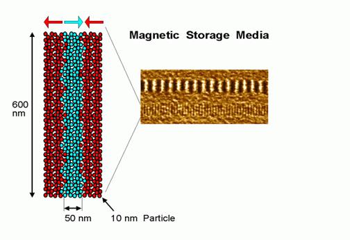
The density limit in magnetic data storage is largely determined by the in homogeneity of the magnetic particles that make up the storage medium. Overcoming variations in particle size, shape, spacing, and magnetic switching currently requires the use of about 100 particles per bit. The error limits are extremely stringent (less than one error in 108 read/write cycles, which can be reduced further to one error in 1012 cycles by error-correcting codes). The individual particles in today's media approach the super paramagnetic limit already (about 10 nm), where thermal fluctuations flip the magnetization.
For further improvements one has to use fewer, but more homogeneous particles. These can be synthesized with great perfection by growing them with a protective surfactant shell. Our current research is aimed at depositing an ordered array of such nano particles onto structured silicon surfaces. The ultimate goal is a single particle per bit memory, which would increase the storage density by a factor of 100
Silicon Memory structure
The new memory was made without the use of lithography as required to make conventional memory chips. To make conventional memory chips, light is used to etch patterns on a chemically treated silicon surface. To use lithography to make chips that are denser than the best available chips is prohibitively expensive and difficult.
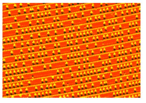
The self-assembled memory structure shown in figures 1 and 2 is obtained by depositing 0.4 monolayer of gold onto a Si(111) surface at 700 ◦C with a post-anneal at 850 ◦C, thereby forming the well-known Si(111)5 × 2–Au structure. All images are taken by STM with a tunneling current of 0.2 nA and a sample bias of −2 V. At this bias the extra silicon atoms are enhanced compared to the underlying 5 × 2 lattice. A stepped Si(111) substrate tilted by 1◦___ towards the azimuth is used to obtain one of the three possible domain orientations exclusively.
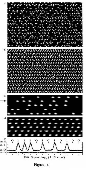
The surface arranges itself into tracks that are exactly five atom rows wide (figure 1). They are oriented parallel to the steps. Protrusions reside on top of the tracks on a 5 × 4 lattice. Only half of the possible sites are occupied in thermal equilibrium (figure 4(a)).When varying the Au coverage the occupancy remains close to 50%. Excess Au is taken up by patches of the Au-rich Si(111)√3 × √3–Au phase, and Au deficiency leads to patches of clean Si(111)7 × 7. In order to find out whether the protrusions are Si or Au, we evaporate additional Si and Au at low temperature (300 ◦C). Silicon fills the vacant sites (figures 4(b) and (d)), but gold does not.
In figure 4(b) the occupancy of the 5 × 4 sites has increased to 90±3% from 53±4% in figure 4(a). Higher annealing allows the extra Si to diffuse away to the nearest step and causes vacancies to reappear, confirming that the half-filled structure is thermodynamically stable. Thus, an average code with 1 and 0 in equal proportion is particularly stable.
Writing is more difficult. While atoms can be positioned controllably at liquid helium temperature, that is much harder to achieve that at room temperature. In order to prevent them from moving around spontaneously it is necessary to choose atoms that are strongly bound to the surface. Pushing them around with the STM tip requires a close approach, which entails the risk of an atom jumping over to the tip. This problem can be turned into a solution by using the STM tip to remove silicon atoms for writing zeros. The memory is pre-formatted with a 1 everywhere by controlled deposition of silicon onto all vacant sites Advantages and Disadvantages
An intriguing aspect of atomic scale memory is that memory density is comparable to the way nature stores data in DNA molecules. The Wisconsin atomic-scale silicon memory uses 20 atoms to store one bit of information, including the space around the single atom bits. DNA uses 32 atoms to store information in one half of the chemical base pair that is the fundamental unit that makes up genetic information. Compared to conventional storage media, both DNA and the silicon surface excel by their storage density. Obviously there are some drawbacks. The memory was constructed and manipulated in a vacuum, and that a scanning tunneling microscope is needed to write memory which makes the writing process very time consuming.
Moreover, there is a tradeoff between memory density and speed. As density increases, the ability to read the memory comes down because we get less and less of a signal. As we make things smaller, it's going to get slower
Conclusion and Future Scope
The push towards the atomic density limit requires a sacrifice in speed. Practical data storage might evolve in a similar direction, with the gain in speed slows down as the density increases. Somewhere on the way to the atomic scale ought to be an optimum combination of density and speed. If the reading and writing speed is improved and the memory is made cost effective, this will revolutionize the field of secondary storage devices. Researchers are working on manufacturing STM with multiple tips or heads that can perform parallel read-write processes.
This type of memory may eventually become useful for storing vast amounts of data, but because the stability of each bit of information depends on one or a few atoms, it likely to be used for applications where a small number of errors can be tolerated
References
. http://www.iop.org/EJ/abstract/0957-4484/13/4/312/
2. http://news.bbc.co.uk/1/hi/sci/tech/2290707.stm
3. http://www.sciencedaily.com/releases
4. The images are from:
Webpage http://www.di.com/movies/movies_inhance/appnotes/odt/odtmain.html
5. http://www.wisc.edu./